Tesla Promises an 80x Chip — in 2029. The Rebrand Is the Real News
Published:
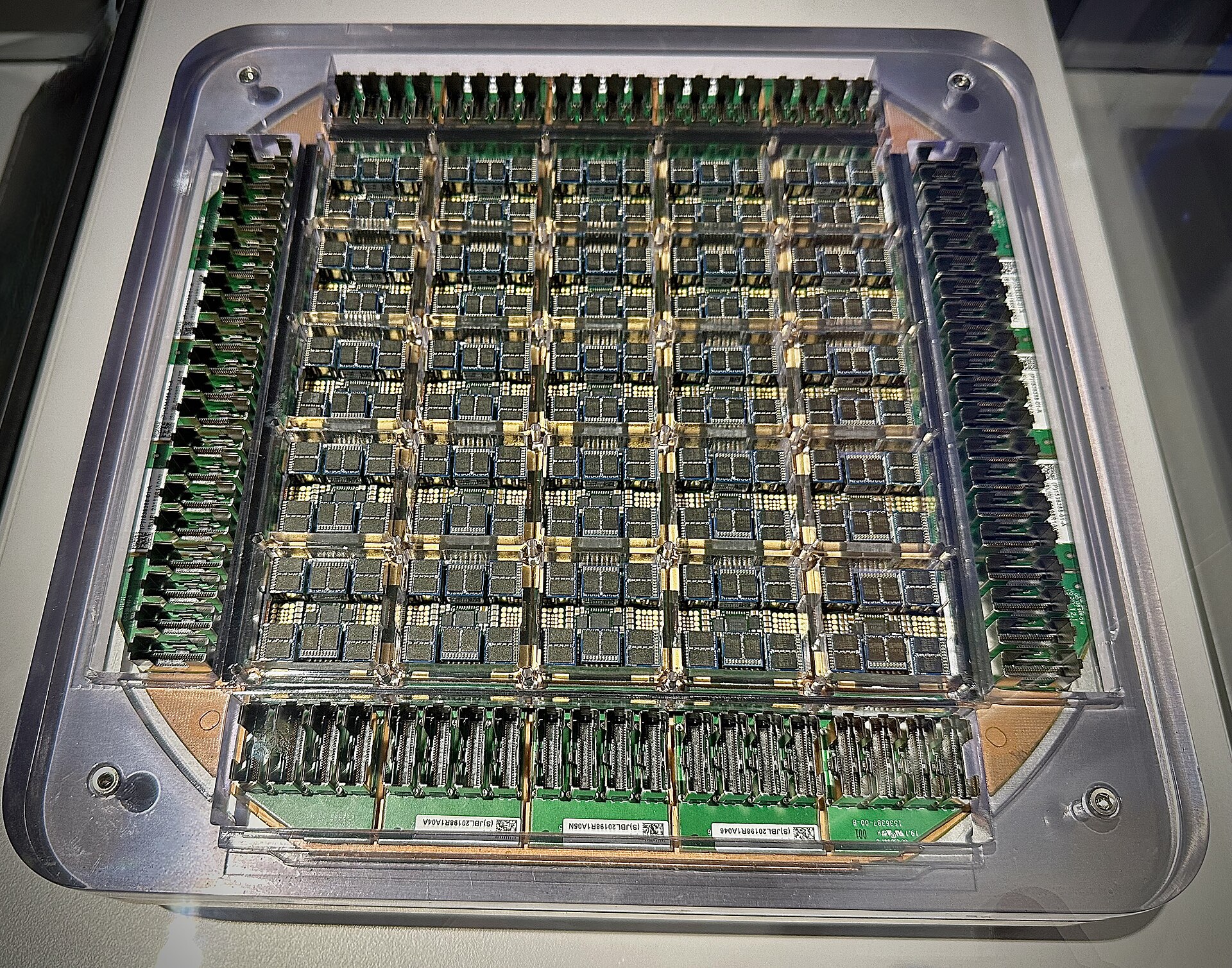
Tesla’s Dojo supercomputer tile — 25 D1 chips on a single wafer-scale tile. Dojo 3 abandons exactly this design. Photo: Wikimedia Commons.
What Tesla disclosed
Tesla has published a revised roadmap for its AI accelerators, and the most visible change is not technical at all: the chips are no longer called AI4, AI5 and AI6. They are SI4, SI5 and SI6 — “SI” for “Super Intelligence,” the term President Trump has pushed as a replacement for “artificial intelligence.” Musk has confirmed the same rebrand for SpaceX’s AI arm, which becomes SpaceXSI.
The headline number belongs to the sixth generation. Tesla says the SI6 inference chip will deliver 80 times the compute of the current fourth-generation chip, SI4, and nine times the memory. On an estimated baseline of 216 to 576 TOPS for the SI4, that works out to roughly 17,280 to 46,080 TOPS — 17 to 46 POPS — with about 144GB of memory, built by Samsung Foundry on a 2nm-class process. The chip is due in 2029–2030, and Tesla has signed an agreement with Samsung to build it through 2033.
The asterisks
Read the numbers carefully, because Tesla itself invites it. The 80x multiple comes from Tesla’s presentation materials. The absolute figures are estimates derived from an estimated SI4 baseline, and Tesla has not disclosed which data formats the SI6 supports — the format is what decides whether a TOPS number means anything in practice. Tesla does not officially disclose absolute compute, memory capacity or power consumption for these chips at all.
So the honest way to state it: Tesla has published a direction, not a product. The validation point is around 2029, and everything between now and then is a claim about a chip that does not exist yet.
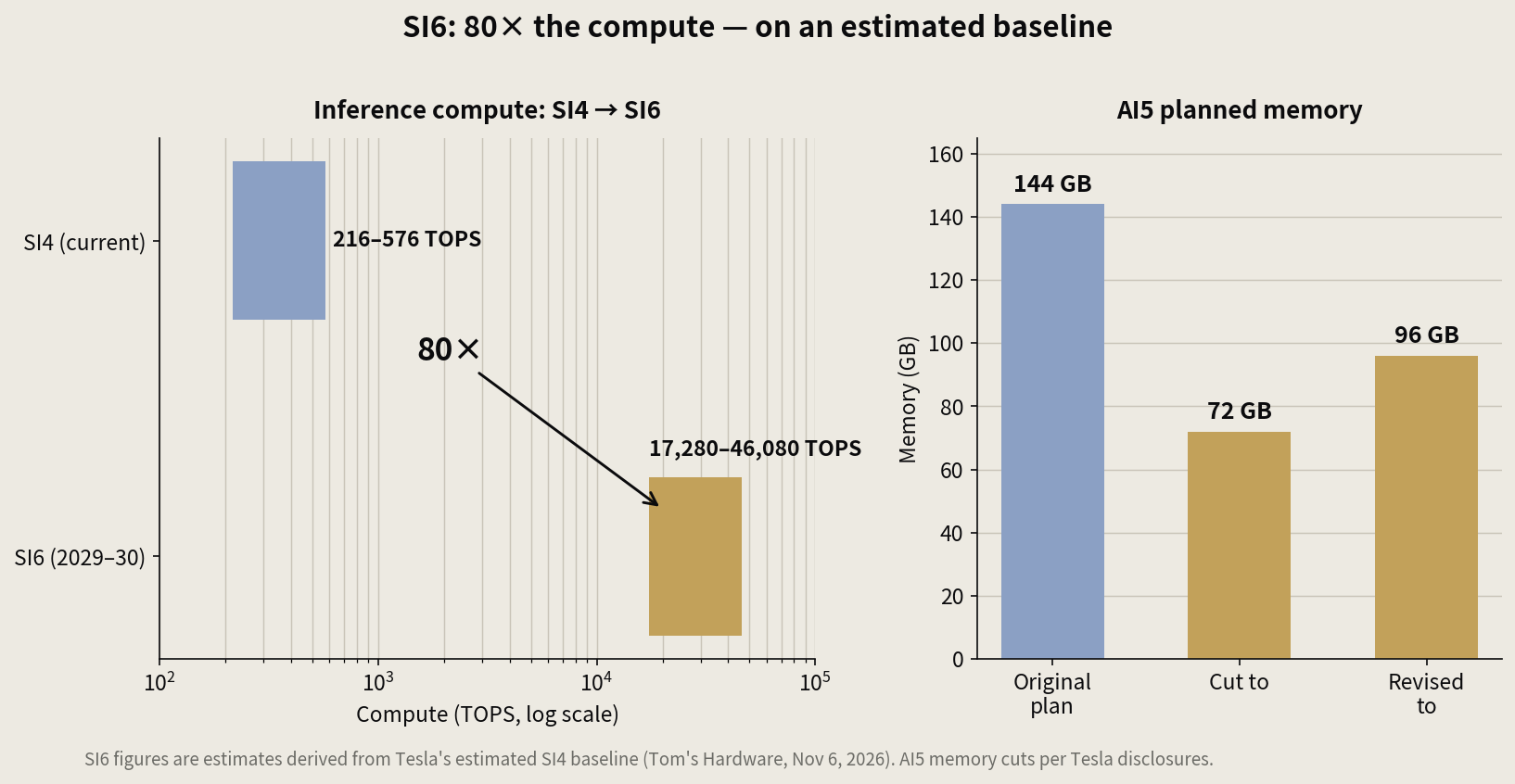
Left: SI6’s 80× compute target against the estimated SI4 baseline (log scale). Right: AI5’s planned memory, cut twice in a month. Chart: this site, from Tesla’s roadmap materials as reported by Tom’s Hardware.
Dojo 3 changes its mind
The more interesting part of the roadmap is the return of Dojo, Tesla’s in-house training accelerator — and it returns as a different machine. The third generation, D3, abandons the wafer-scale integration and distributed on-chip SRAM architecture that defined the first two generations, shifting instead to a chiplet-based design with 2.5D and 3D packaging and stacked HBM memory.
That is a genuine U-turn. Wafer-scale integration was Dojo’s identity — the bet that one giant wafer of compute beats many small chips wired together. D3 concedes the point the rest of the industry settled years ago: chiplets and stacked memory win. Tesla disclosed no compute, memory, process or schedule for D3, so the scale of the concession is still unknown. But the direction is unmistakable, and it is the opposite of the original Dojo pitch.
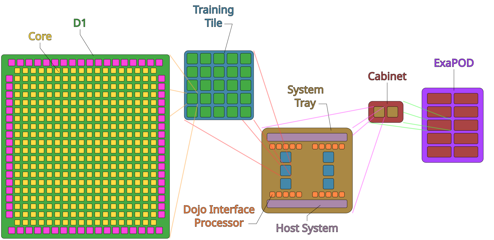
The original Dojo architecture, from a single D1 chip up to an ExaPOD — wafer-scale integration and distributed on-chip SRAM. D3 drops both. Diagram: Wikimedia Commons.
The memory irony
There is a tension inside Tesla’s own roadmap that the company did not volunteer. Just last month, Musk cut the planned memory on the AI5 chip from 144GB to 72GB, then to 96GB, to secure enough chip supply for volume Optimus production — a public, real-time negotiation with the memory shortage that is squeezing the whole industry. AI5 is in trial production at Samsung’s Taylor, Texas facility, with larger-scale production targeted for 2027 and Optimus integration around April 2027.
In other words: the chip Tesla can actually ship next is the one whose memory it just cut twice, while the chip with nine times the memory is a 2029–2030 target. Roadmaps are cheap. Memory supply is not.
The judgment
The SI6 announcement is best read as three separate stories. The rebrand is politics, and it is already done — “Super Intelligence” is now the house style across Musk’s companies. The Dojo 3 pivot is engineering, and it is the most honest part of the roadmap: Tesla admitting its signature architecture lost. The 80x is marketing, and it will stay marketing until a real chip exists to measure.
None of that makes the roadmap meaningless. A car company that designs its own training and inference silicon, with a Samsung foundry agreement running to 2033, is a serious vertical bet — the same bet that underpins the robotaxi and Optimus programs. But the number to remember is not 80. It is 2029. Until then, Tesla’s chip story is a promise competing with a memory market that just forced it to cut its next chip in half.
Roadmap figures in this post are from Tesla presentation materials as reported by Tom’s Hardware, November 6, 2026; absolute compute figures are estimates derived from the SI4 baseline, as the underlying reporting notes.
Share on
Twitter Facebook LinkedIn☕ Buy me a coffee! 💝
If you found this article helpful, consider buying me a coffee to support my work! 🚀